Semiconductor
Introduction to Semiconductors
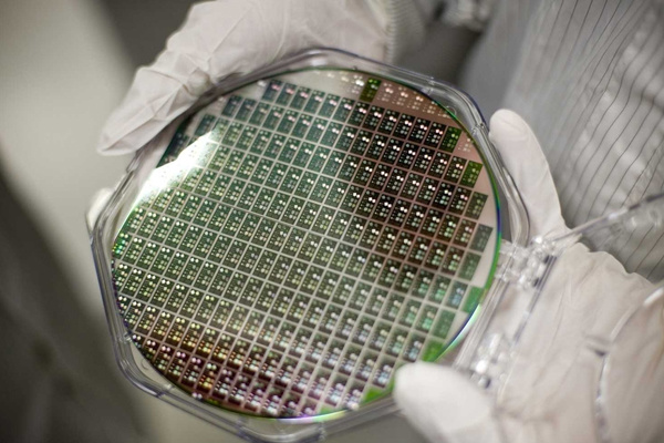
A semiconductor refers to a material whose electrical conductivity is between that of a conductor and an insulator at room temperature.
Semiconductors are used in integrated circuits, consumer electronics, communication systems, photovoltaic power generation, lighting, high-power power conversion and other fields. For example, diodes are devices made of semiconductors.
Whether from the perspective of technology or economic development, the importance of semiconductors is very huge. The core units of most electronic products, such as computers, mobile phones or digital recorders, are closely related to semiconductors.
Common semiconductor materials include silicon, germanium, gallium arsenide, etc. Silicon is the most influential one in the application of various semiconductor materials.
First Generation Semiconductor
It mainly refers to elemental semiconductor materials represented by silicon (Si) and germanium (Ge), which are widely used, including integrated circuits, electronic information network engineering, computers, mobile phones, etc. Among them, the most typical application is integrated circuits, which are mainly used in low-voltage, low-frequency, low-power transistors and detectors, replacing bulky electron tubes, leading to the possibility of integrated circuits.
Second Generation Semiconductors
It is mainly compound materials represented by gallium arsenide (GaAs) and indium phosphide (InP), which are mainly used in millimeter-wave devices and light-emitting devices. Satellite communication, mobile communication, optical communication, GPS navigation, etc. It has good material properties such as electron mobility and band gap, and is scarce in resources, toxic and polluting the environment.
Third-generation Semiconductors
Refers to broadband semiconductor materials represented by silicon carbide (SiC), gallium nitride (GaN), zinc oxide (ZnO), diamond, and aluminum nitride (AlN), with better electron mobility, band gap, and breakdown voltage. , high temperature, high frequency, anti-radiation, high-power devices and other characteristics. It is mostly used in communications, new energy vehicles, high-speed rail, satellite communications, aerospace and other scenarios, among which the research and development of silicon carbide and gallium nitride are relatively mature.
Production Process Flow Of Semiconductor Wafers
Crystal Growth ➤ Shaping ➤ Slicing ➤ Grinding/Chamfering ➤ Etching ➤ Polishing ➤ Cleaning ➤ Inspection ➤ Packaging
Yuhuan Can Be Used As Process Section
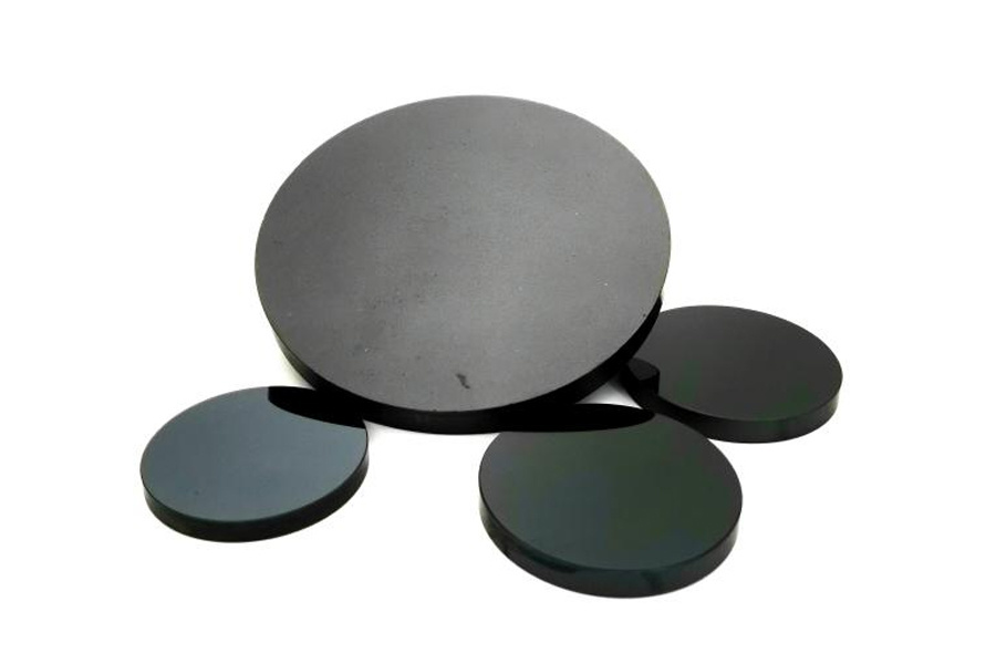

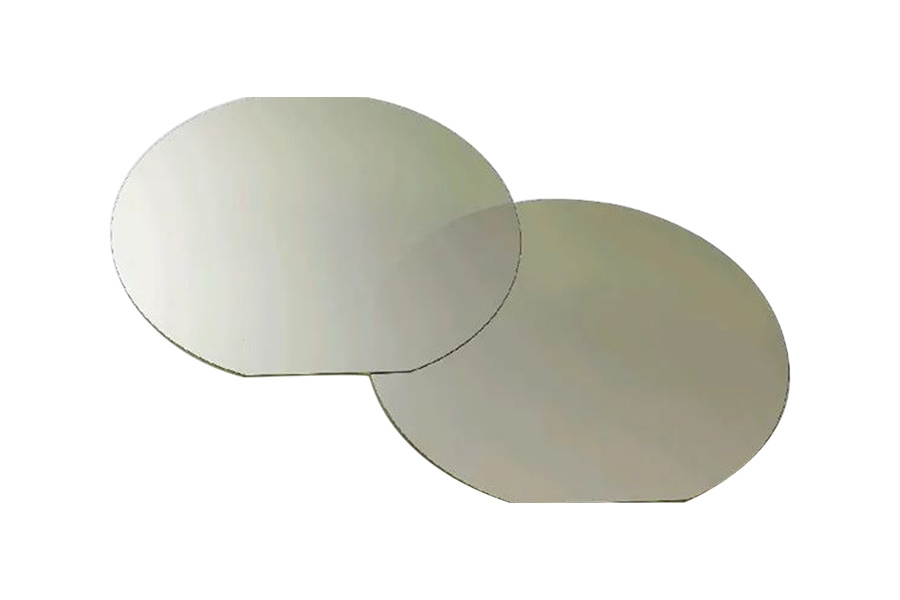

Yuhuan Applicable Equipment
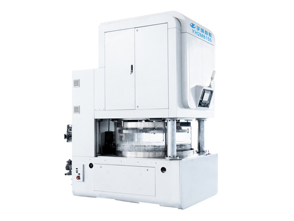

Main Process :
CMP (Chemical Mechanical Polishing, chemical mechanical polishing)
Rough polishing: Magnesium oxide is generally used for rough polishing. The purpose is to remove the residual mechanical damage on the surface of the silicon wafer. Generally, it is required to remove 20~30μm from the surface.
Fine polishing: Fine polishing is performed with silicon dioxide. The purpose is to remove the slight damage and cloud-like defects left by the first polishing on the surface of the silicon wafer, and a thickness of 2-3 μm is required to be removed from the surface.
